

Electronics (ECAD) — KiCad and Altium schematic and PCB, tied to PLM
Open a KiCad or Altium schematic and board in PORTWARE; every part leads to its PLM part and lifecycle, a board's nets light up, two revisions are compared and a new revision writes down what changed.
- KiCad and AltiumKiCad files, Altium schematics and boards and Eagle boards open in the same place.
- Tied to PLMA part's MPN leads to its PLM part and lifecycle; parts at risk are marked.
- Revision compareParts and nets added, removed, changed; the earlier drawing a click away.
- Changes written downA new revision writes its change list into the part's chatter.
Where it appears: PLM › Electronics › ECAD documents · the ECAD Workbench button on the document
Electronics design files are PLM documents. Schematics, PCB layouts, projects, libraries and Gerber/drill files are recognised by their extension and listed by kind.
ECAD Workbench
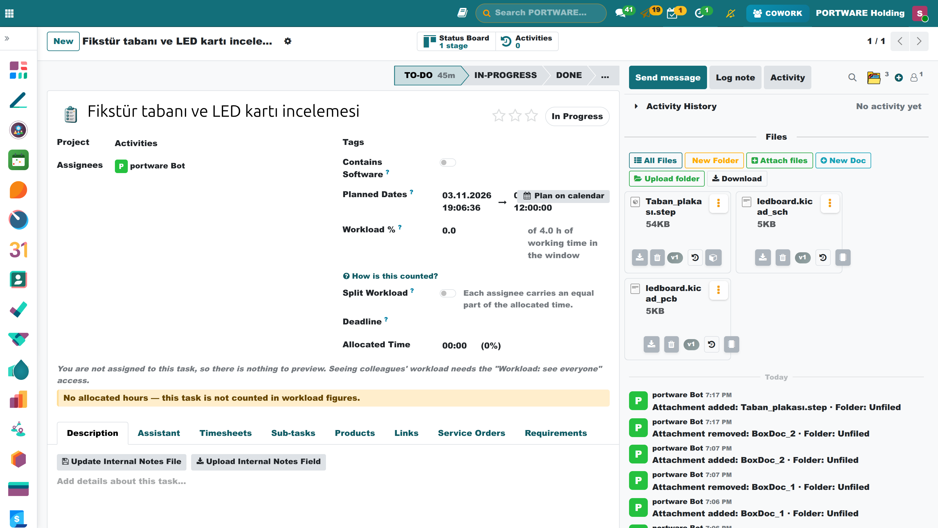
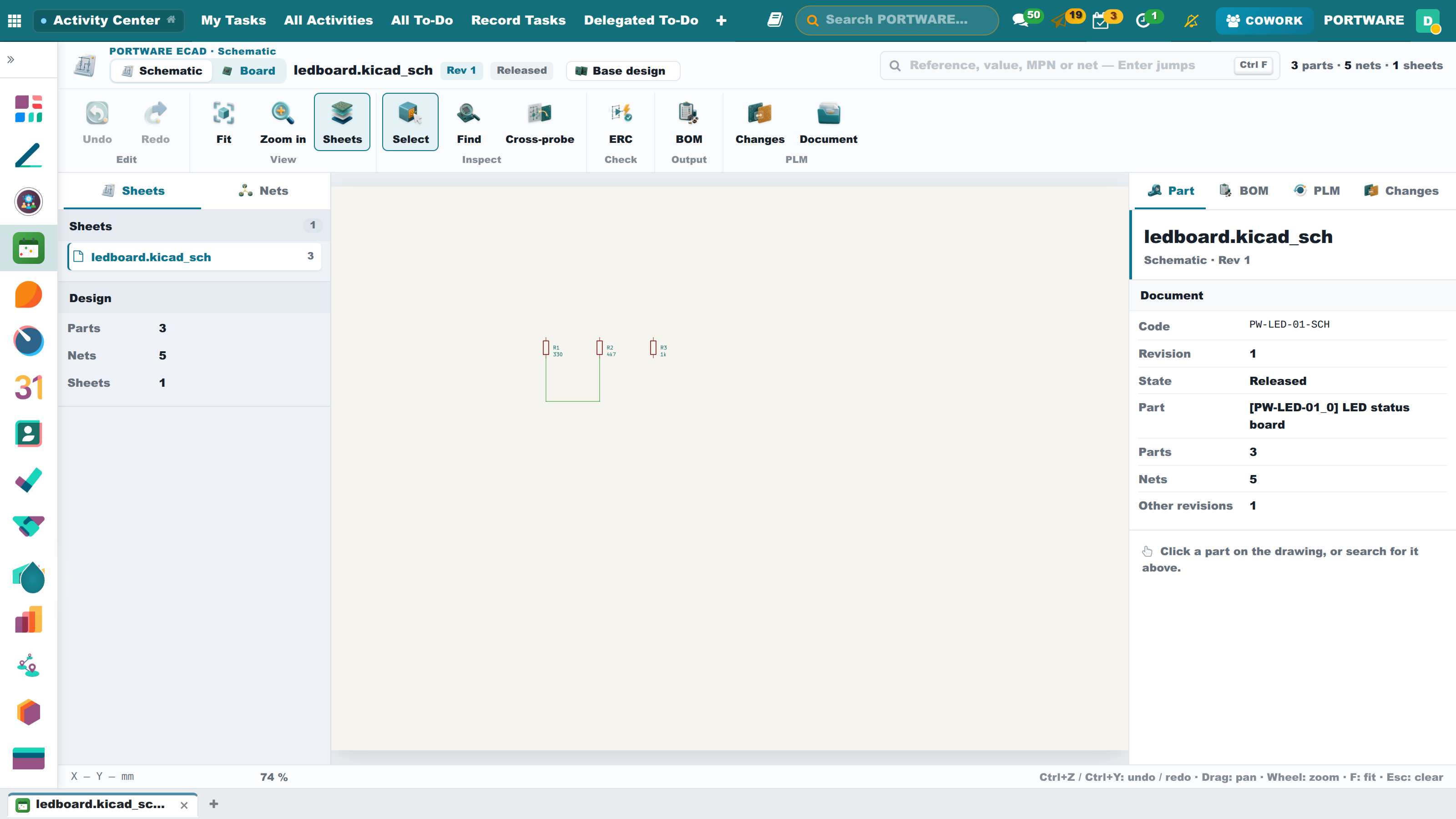
Press ECAD Workbench on a KiCad schematic (.kicad_sch) or board (.kicad_pcb), an Altium schematic (.SchDoc) or board (.PcbDoc), or an Eagle board (.brd). When such a file is attached to a task, a product or a chat, Open in the ECAD workbench (the chip button on its card) opens the same workbench in a new tab.
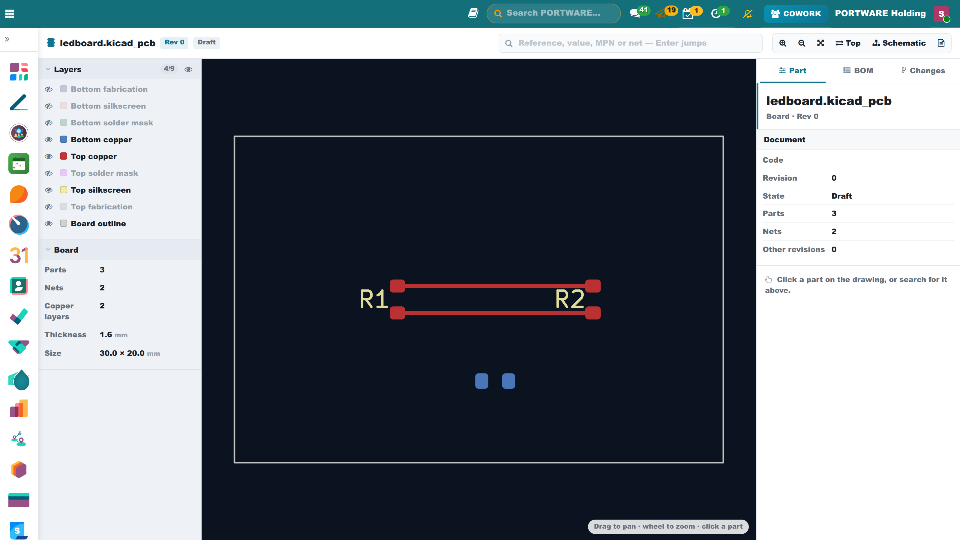
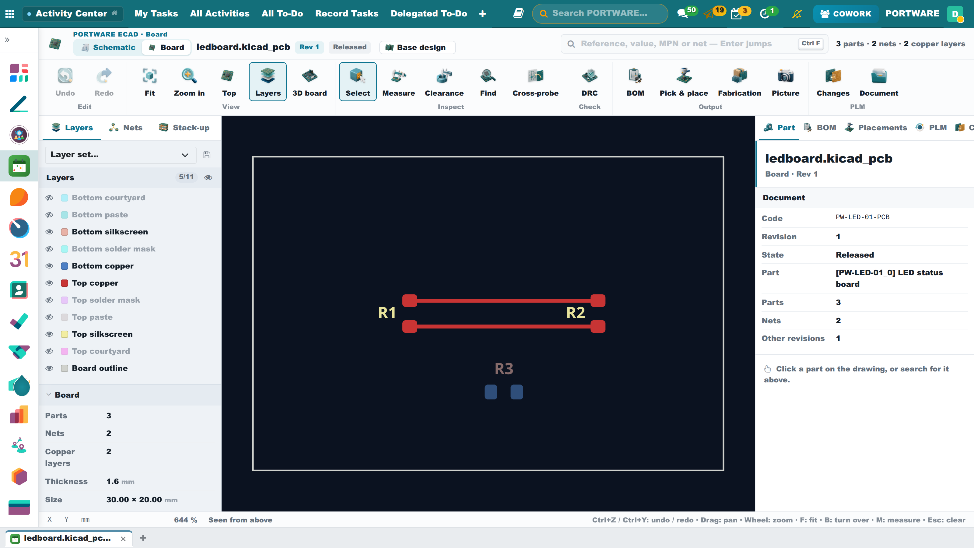
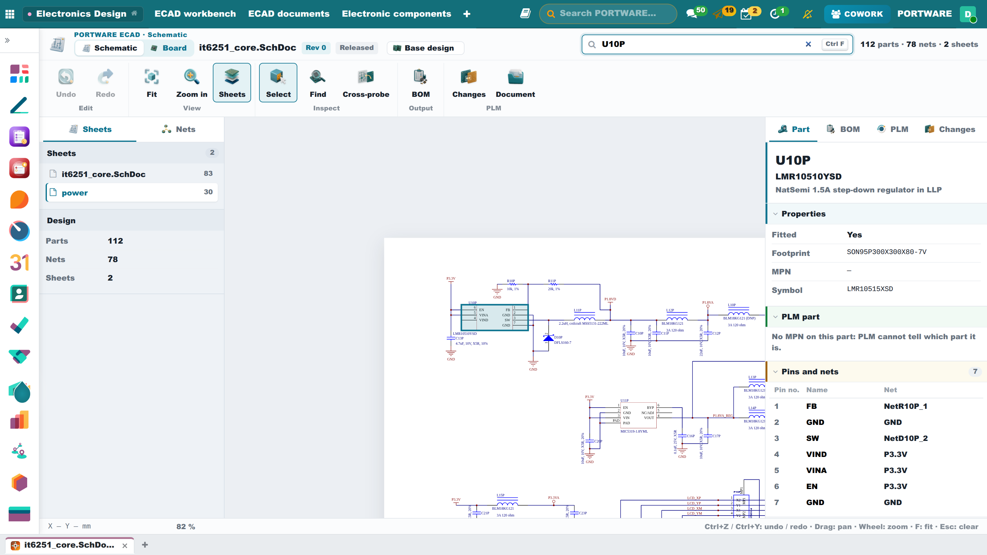
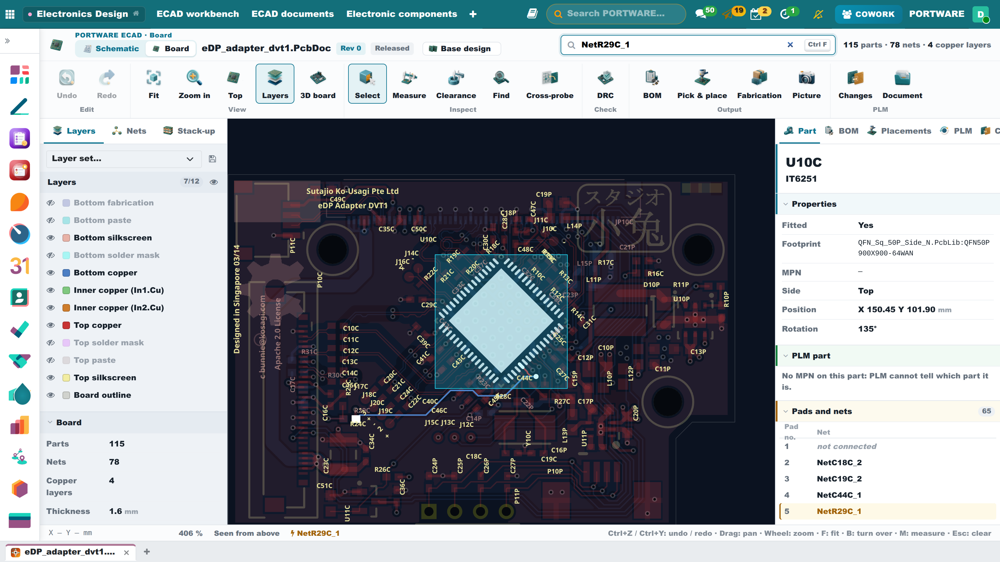
- The drawing. KiCad draws a KiCad file, so it is exactly what the designer sees. For Altium files, see the section below. Every sheet of the schematic is listed on the left. The board's layers (copper, silkscreen, mask, board outline) switch on and off one by one, and Top / Bottom shows the board from below. Drag to pan and use the wheel to zoom; the drawing stays sharp at every zoom.
- Finding a part. Type a reference, value, MPN or net name in the search box; Enter goes to the part. Clicking a part on the drawing also picks it.
- Panels. The screen is laid out like an engineering desk: the navigator on the left (sheets or layers, design and board facts), the Properties inspector on the right. Sections fold from their headers. With nothing picked, the inspector describes the document: its code, revision, state, parts and nets.
- The part card. The picked part's reference and value sit at the top on a coloured strip that tells its state (known to PLM, at risk, obsolete, not fitted). Below, the footprint, MPN, symbol, board side, position and rotation and the other schematic fields line up in a property table.
- Pins and nets. The picked part's pins (schematic) or pads (board) are listed with their nets. A click on a row brings the net forward and steps the rest of the drawing back: on a board every pad and track of the net lights, on a schematic every part the net joins is marked. A net name can also be found from the search box.
- Layers. Every layer has an eye and its colour; Only this layer shows it alone with the board outline, and a second click brings every layer back.
- The PLM part. When the MPN is on an approved manufacturer list (AML), the card shows the PLM part, its revision and its lifecycle (active, not for new designs, last-time buy, obsolete). A click on the card opens the product.
- BOM. The BOM tab groups the design's parts by value, footprint and MPN. Each line shows the quantity and references, what PLM knows of it, and a risk mark. The figures at the top count parts, lines, lines in PLM and lines at risk.
- Schematic ↔ board. The Schematic | Board tabs in the header switch between the two halves of the design in one click; the picked part or net is picked on the other side too. Schematic and board are found the way the ECAD tools tie them: the Altium project's (
.PrjPcb) document list, KiCad's shared project name and sub-sheet references, or the files on one record. No part needs to be linked.
The drawing and the facts read from the design are prepared once and kept beside the document. They are prepared again when the file's content changes.
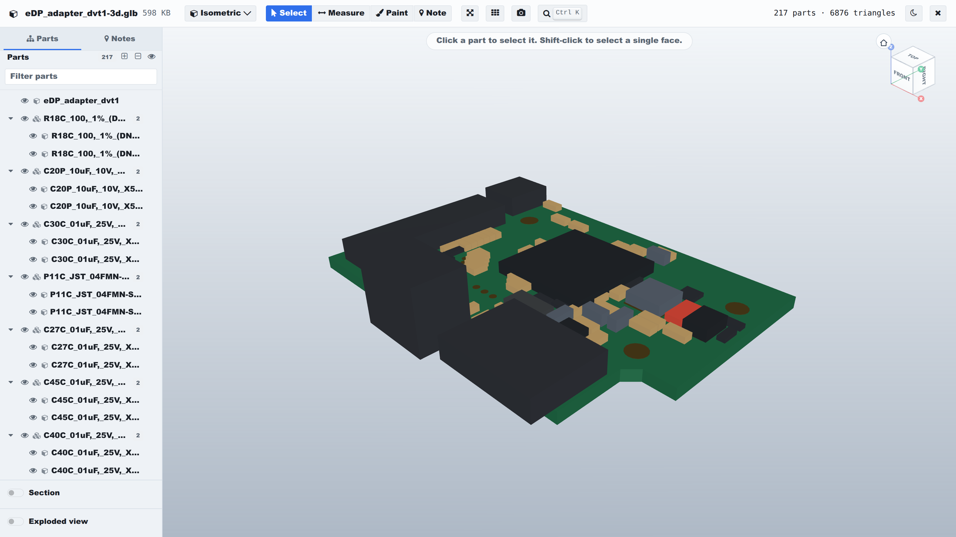
The board in 3D
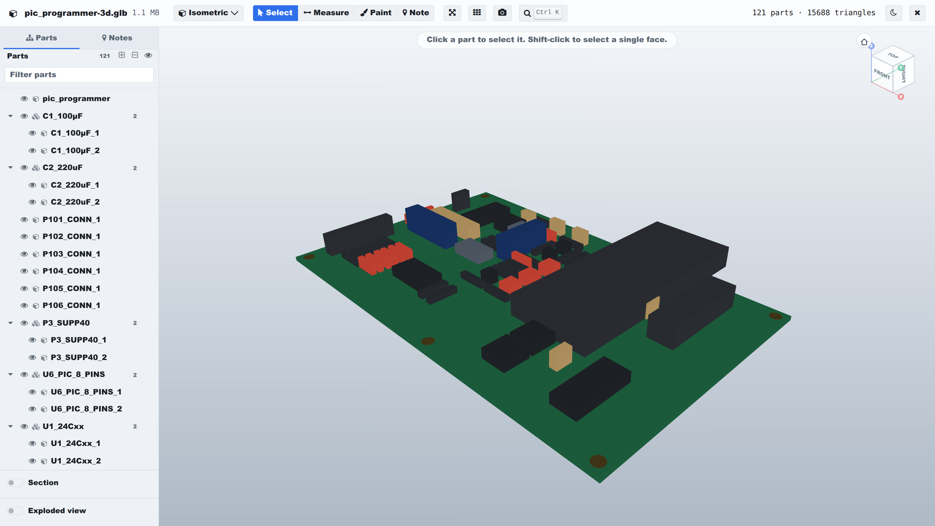
On a board (KiCad, Altium or Eagle), 3D view opens it in the 3D viewer. The outline is drawn at its true thickness in green solder mask, the pads in gold. Every part becomes a body over its footprint, as tall and coloured as its kind: ICs black, resistors and capacitors flat, electrolytics blue and tall, LEDs red, connectors high. Mounting holes have no body. The parts tree lists every part by reference and value; section, measure and explode work. The model is kept in PLM beside the board as its -3d.glb output. No 3D component library is needed; it serves mechanical checks and enclosure design.
Altium and Eagle
Most customers design in Altium Designer. Altium files are uploaded as PLM documents as they are, without converting them.
- Altium schematic (
.SchDoc). PORTWARE reads and draws the file itself, in the designer's colours and fonts, with its pins, power symbols, ports and sheet symbols. Every sheet of the project is listed on the left: the sheet symbols of a hierarchical design, or the project file (.PrjPcb) of a flat one, give the order. The nets come out as Altium compiles them; a part of several units (U1A, U1B) counts as one part. - Altium board (
.PcbDoc, CircuitStudio, CircuitMaker) and Eagle board (.brd). Read on the server with KiCad's own importer, then handled like a KiCad board: layers, picking a part, lighting a net, revision compare. Generate outputs makes their STEP, SVG and Gerber/drill set too. - BOM. On an Altium schematic, Import BOM hands its parts to the import wizard in Altium's own BOM CSV form.
- The design stays whole. When only one sheet gets a new revision, the other sheets are read as they stood when that revision was uploaded. The change note lists only the parts of the sheet that really changed.
Revision compare and change tracking
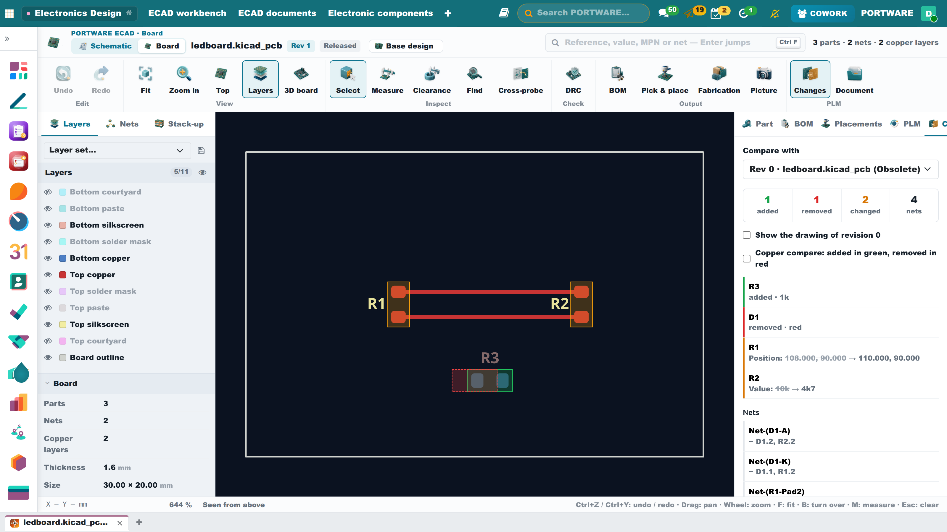
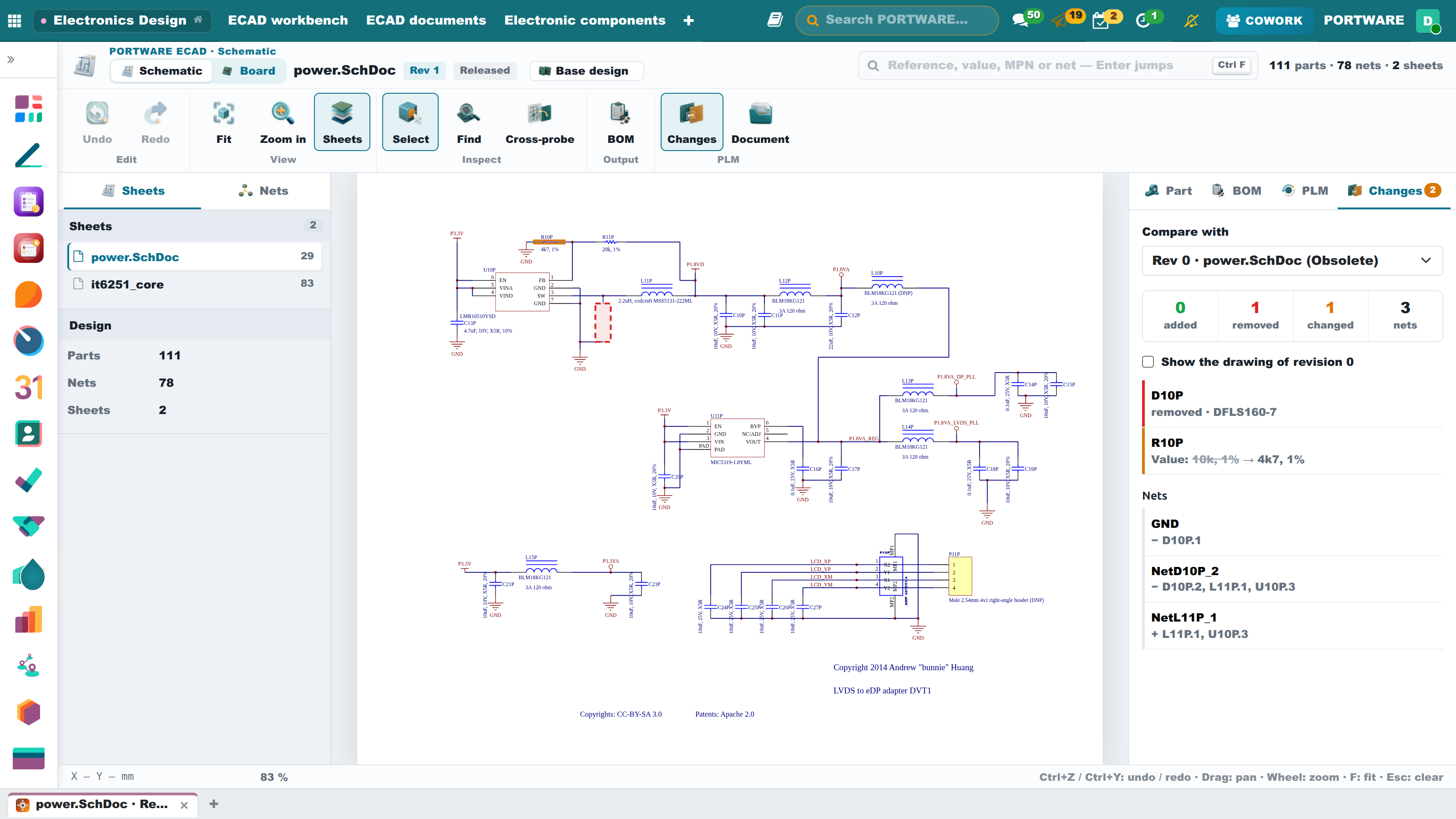
On the Changes tab, pick another revision of the same document. The compare finds:
- parts added and removed;
- parts whose value, footprint, MPN or not-fitted flag changed;
- parts moved, turned or flipped to the other side of the board;
- nets whose pins changed. A net with the same pins under a new name shows as renamed, not as one net lost and another found.
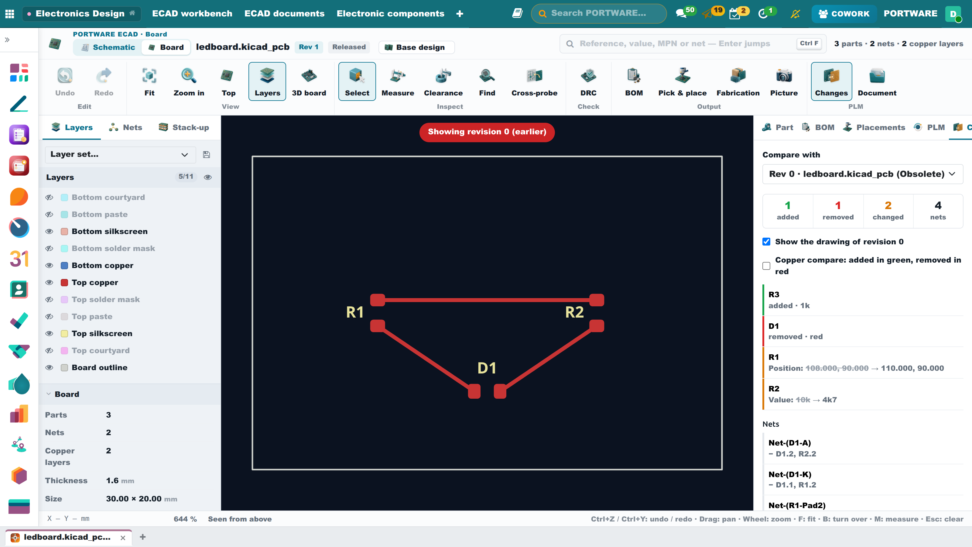
The changed parts are coloured on the drawing: added green, changed amber, removed in red dashes where they used to be. Show the drawing of revision N brings the earlier drawing into the same place, so the two revisions can be compared one over the other.
When a new file is uploaded to a new revision of a KiCad or Altium document, the change list is made on its own. It is written into the document's Changes against the previous revision field and into its part's chatter. Whoever approves the change order reads there what changed.
Electronic BOM import
A KiCad XML BOM, an IPC-2581 file, or an Altium, OrCAD, EasyEDA or distributor CSV becomes the board's engineering BOM. Each component is one line and keeps its references. Parts are found by MPN through the approved manufacturer list; missing ones are created. Before anything is written, the import shows what changes against the current BOM. A released board's BOM does not change; that goes through a new revision.
KiCad outputs and Gerber
Generate outputs runs KiCad on the server:
- from a schematic: its PDF and BOM;
- from a board: its STEP (it opens in the 3D viewer), SVG and Gerber/drill set.
They all become PLM documents linked to the same parts. The Gerber Viewer draws a Gerber/drill set layer by layer, from the top or the bottom.
Design Checks, Measuring and Variants
- An app of its own. Electronics Design sits on the home screen beside 3D Design.
- Cross-probing. The board opens beside its schematic (or the reverse); the selected part and net light up on both.
- Measure and clearance. Distances on the board and clearance between conductors are measured with snapping, as in KiCad.
- DRC and ERC. Design and electrical rules are checked on the server by KiCad. Findings are listed in the workbench and the report is filed in PLM.
- Variants. Altium project variants are read into PLM. Each variant's BOM and pick-and-place list come out separately and download as CSV.
- Gerber compare and Add to PLM. Two Gerber sets are compared layer by layer; a design file attached anywhere becomes a PLM document in one click.
Safety
Files are read with size and depth limits. The drawings are shown as pictures only; nothing in them can run. Every request runs with the reader's own access, and only revisions of the same document are compared.
| Module | What it does | Version |
|---|---|---|
| PORTWARE PLM ECAD | Electronics in PLM: component data, approved manufacturers, schematic/PCB documents and electronic BOM import | 19.0.7.2.1 live |